sekar
quite active
Posts: 161 
|
Post by sekar on Jun 19, 2016 20:36:43 GMT
Hi, Chris . It's new interesting project. You may use high speed rotary tool like Dremel ( as most expensive ) to cut holes/slots in your alu case or totally change it's shape  . There are a lot of different accessories for different tasks. I forgot about tinkering with different files since i began to work with a mini drill. Hi Sergey, yes it is definitely an interesting project (thanks to Frans) - so when are we going to see your version?  I have a rotary tool similar to the Dremel but I never use it. I prefer to use a hand file and gently remove a little bit at a time, experience has taught me that you can always file a little bit more off but you cannot add a little bit back on  When I use a power tool I nearly always take off too much. Chris, I suppose to get back to my mountain bike to correct my health just now. It's more important for me. I need some refreshment and to keep ( rather to begin ) active style  , so - NO tinkering and soldering but rolling pedals. Sorry for omitting "a" and "the" articles .... |
|
Crispy
very active
Madrigal music is playing - Voices can faintly be heard, "Please leave this patient undisturbed."
Posts: 779 
|
Post by Crispy on Jun 20, 2016 12:21:02 GMT
Yes, the bottom slot (yellow arrow). I didn't make that very clear in the manual... will take some pictures and add them later on in the manual. You can use this one if you like? 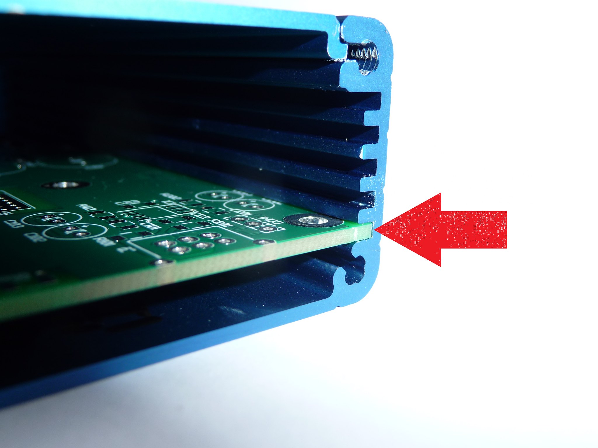 I have found another thing you may want to amend in the manual when you add the pictures. Page 19 The Beyer DT770 pro 250 ohms filter table is showing exactly the same table as the Audio Technica ATH-M40X filter module above it. Because my DT770 pro's are 80ohms - just wandered if there was a filter for them or would the 250ohm version work? The metal work is the hardest part (also making the holes of the front plate on the exact positions. You can smuggle a bit on the volpot hole and the 6.3 mm output jack hole as they are covered by a large nut and the volpot knob. You do need to line up the LED holes neatly when they are positioned closely together. I am not quite going to do it the same as you Frans and I am considering doing it like this?  I want to use a 3.5mm jack and place the two LEDs in the middle of the jack and the vol pot. The pic below shows how I think it should be wired up? - do I need to jumper over the wires to the other side of the board on con 2. 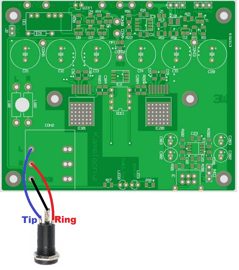 I must say the quality of the PCB board is first class and I am going to attempt to put some SMD resistors on to it this afternoon  For anybody who is interested in my arrangement of the back plate the measurements are: 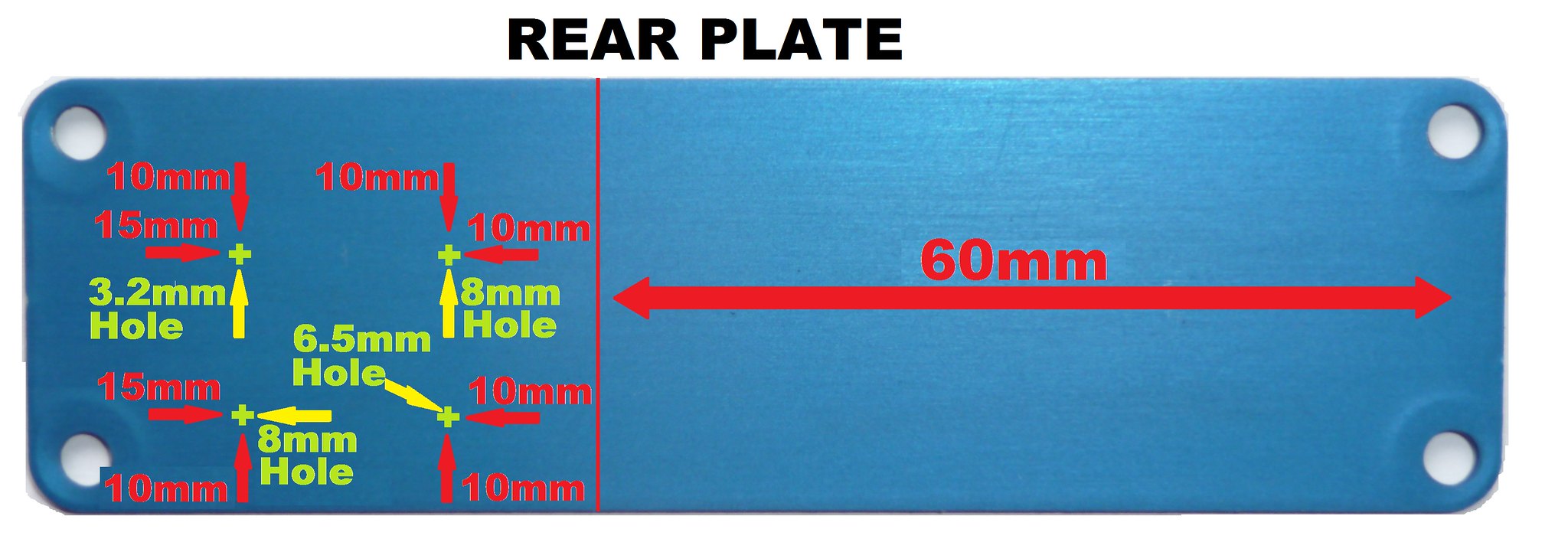 |
|
solderdude
Administrator
measureutternutter
Posts: 4,886
|
Post by solderdude on Jun 20, 2016 14:30:23 GMT
I used the 6.3 mm so you can use 3.5mm (in an adapter) and 6.3mm.
When using a 3.5mm as output jack you will have to use a converter cord.
connecting the 3.5mm socket is correct as shown.
No need to jumper any wires.
Soldering SMD is quite do-able.
There are tips for soldering in the article and when you follow those it is quite easy to solder them on.
Make sure the solder flows nicely.
|
|
Crispy
very active
Madrigal music is playing - Voices can faintly be heard, "Please leave this patient undisturbed."
Posts: 779 
|
Post by Crispy on Jun 21, 2016 7:30:15 GMT
Soldering SMD is quite do-able. There are tips for soldering in the article and when you follow those it is quite easy to solder them on. Make sure the solder flows nicely. Yes that part of the manual is very very helpful Frans and a picture paints a thousand words. I spent yesterday afternoon soldering and managed to get quite a bit done - Resistors in place (easy)  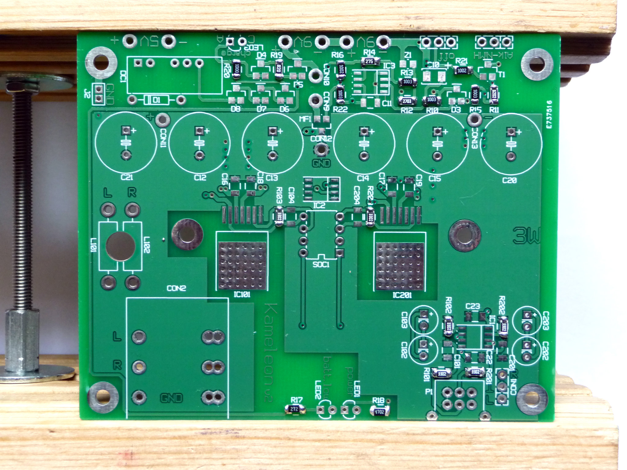 I then got carried away and put in 99% of the caps and for some reason could not find C10 - it will be in my box somewhere just need to find it. I also put in D1 to D8 and for the life of me cannot find D9 on the board, the parts list says (5, BAS19) D3,D6,D7,D8 & D9. Could you point out where it is on the board please, I was probably tired and could not see the wood for the trees? Resitors, Caps and a few other components in place: 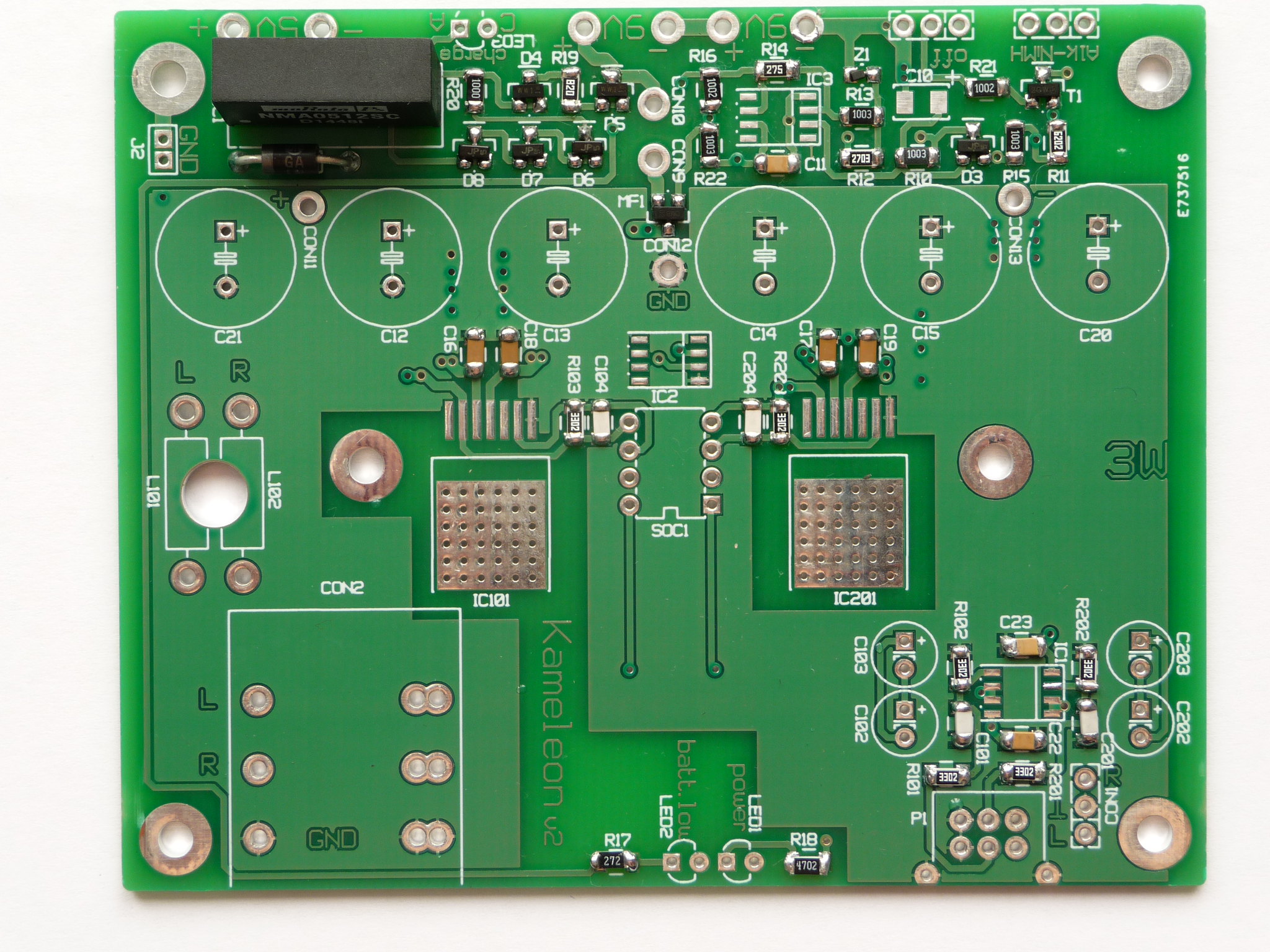 Next problem was Z1, I honestly thought I had broken it getting it out of the strip it was that small, I also had a real problem seeing it to solder let alone see any markings and it was only by pure look I noticed a stripe on one side. After a quick look at the schematic I guessed from it that the stripe should be as below? is this correct. 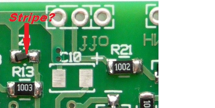 I am also having a problem with IC3 that you sent me, after a quick clean up of the part I noticed the small dot that indicates pin 1, but where does pin 1 go on the board? I have marked on the pic below where I think it might go, is this correct? 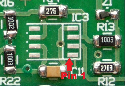 One last thing, Page 5 of the manual Parts List shows R101, R202 (Should be R102?) R201, R202, R103, R203 |
|
solderdude
Administrator
measureutternutter
Posts: 4,886
|
Post by solderdude on Jun 21, 2016 7:58:40 GMT
You found another error in the parts list.
D9 does not exist.
Will update the manual when I have some time.
The stripe of R13 is correct, it is mounted as it should.
When powering it up you should measure 5.6V across it, when it measures 0.6V it is mounted the wrong way.
They are hard to solder indeed but these are the only very low current (battery operated) zeners.
The larger ones all need substantially higher currents to operate.
Pin1 on IC3 is near the C11 markings.
IC1 has the same orientation (pin1 is near C22)
The stripe in the silkscreen marks the 'slanted' section of the physical part.
On the slanted side you find pins 1 to 4.
Not all components have a slanted side though, some have a dot near pin 1.
Yes, the first R202 should say R102, yet another thing I have to correct.
Should check the desktop manual as well as some of the parts lists are (part) copies.
I recommend to build the power supply section first and not yet fit IC1, IC101 and IC201 yet (all the other parts can be fitted) and test the power supply part.
The rail splitter and low batttery voltage/charging section.
Easier to debug that circuit when there is no amp section yet.
Once the +/-9V is there you can finish the board by adding those 3 IC's.
|
|
Crispy
very active
Madrigal music is playing - Voices can faintly be heard, "Please leave this patient undisturbed."
Posts: 779 
|
Post by Crispy on Jun 21, 2016 20:24:24 GMT
You found another error in the parts list. D9 does not exist. Yes, the first R202 should say R102, yet another thing I have to correct. Should check the desktop manual as well as some of the parts lists are (part) copies. Will update the manual when I have some time. I bet you wish I had never started this project - all the extra work I am causing you  Pin1 on IC3 is near the C11 markings. IC1 has the same orientation (pin1 is near C22) The stripe in the silkscreen marks the 'slanted' section of the physical part. On the slanted side you find pins 1 to 4. Not all components have a slanted side though, some have a dot near pin 1. I am still totally confused with these? I have took some pics if they can help you to help me identify the correct orientation; IC3: Pin one yellow or red or is it at the opposite side? 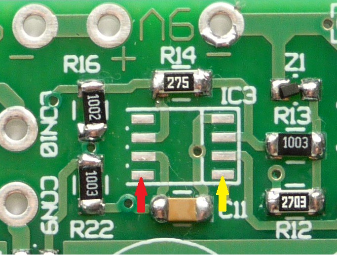 IC2 board: Pin one yellow or red? 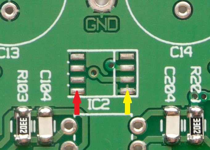 IC1 board:Pin one yellow or red? 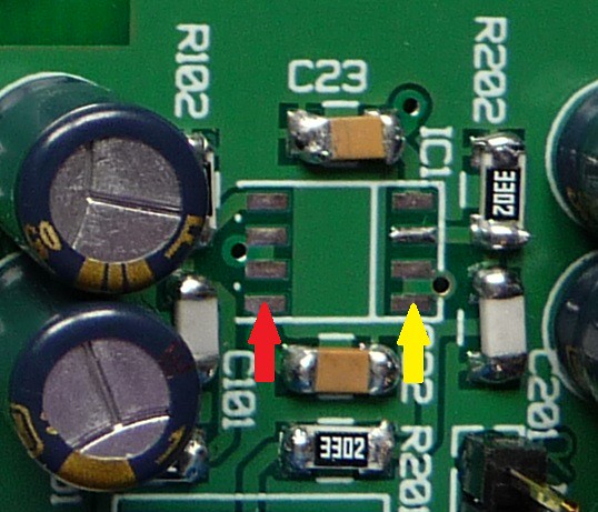
I think I have found C10? Pic below
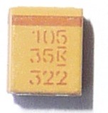 Now if I am correct and done my homework this cap is polar and the brown stripe indicates +? If this is correct then I also think that this is worth a mention in the manual as it states the SMD caps have no markings along with Z1 orientation which is very very easy to miss, just for non electrical guys like myself. (I have just had another look at the board and noticed there is a + sign on the right side of C10, so I am assuming I am correct?) |
|
solderdude
Administrator
measureutternutter
Posts: 4,886
|
Post by solderdude on Jun 21, 2016 22:05:22 GMT
SMD caps:  The stripe is the + which is marked on the PCB. On your PCB pictures the red arrow = pin 8 and the yellow arrow = pin 1 Pin 1 on an SO-8 IC is either indicated by the slanted area:   or by a dot (depends on manufacturer)  or by both (slanted area + dot)  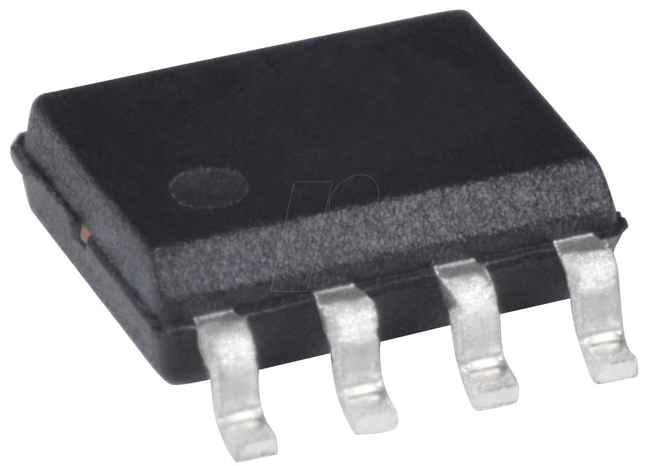 |
|
juke
very active
Posts: 396 
|
Post by juke on Jun 22, 2016 9:17:01 GMT
I don't understand the Ta-pearl part of the pic, two positives?
I thought all of that shape could be inserted either way round.
Syd
|
|
solderdude
Administrator
measureutternutter
Posts: 4,886
|
Post by solderdude on Jun 22, 2016 9:57:06 GMT
All tantalum capacitors are polar. The Ta-pearl is no exception, they are all polar. In fact the (wet) aluminium capacitor can handle some negative voltage but the tantalum, being a semiconductor, can't and developpes a short when a reverse voltage is applied. Some tanatalums have a single + printed on one side, some a stripe and others a + and a stripe or a row of +'s indicating the pin closest to it. Strangely enough wet, as well as solid, aluminum electrolytic capacitors, diodes and zeners have a stripe indicating the negative side where tantalum capacitors have a stripe indicating the positive pin. No idea why that is though... we just have to learn to live with that I suppose. Solid Aluminium caps look a lot like the Ta pearl caps so can be very confusing. There are ceramic multilayer caps that look a lot like tanatlums in color and material but are usually 'flat' and not cylindrical like tantalums. Ceramic multilayers are non polar and can be fitted either way around. tantalum: 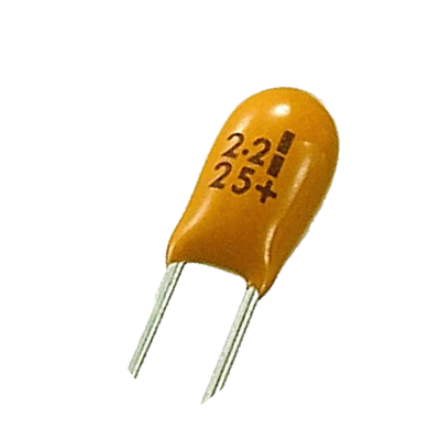 and ceramic multilayer:  |
|
Crispy
very active
Madrigal music is playing - Voices can faintly be heard, "Please leave this patient undisturbed."
Posts: 779 
|
Post by Crispy on Jun 22, 2016 19:41:57 GMT
On your PCB pictures the red arrow = pin 8 and the yellow arrow = pin 1 Thanks Frans that has cleared up that little problem  Pin 1 on an SO-8 IC is either indicated by the slanted area:  or by a dot (depends on manufacturer)  OK next problem: I took out IC1, IC2 & IC3 and had a good look at them with stronger glasses and a magnifying glass. IC1 is no problem and it has a dot indicating pin one  IC1 & IC2 are like the stock picture below. 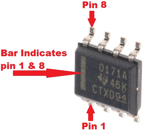 IC3 the one that you sent me is like this: 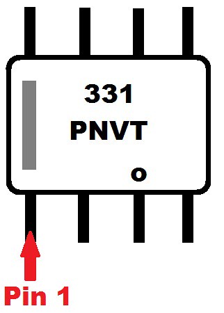 It has the same bar on the left and the top 331? marking was obscured - the rest PNVT was readable with either a small zero or dot as in the picture. So I am still at a loss as to which is pin one on these two IC's  so I hope this sheds some light on the matter so I can get IC2 & 3 soldered in place as it stresses that they MUST not be soldered on the WRONG way. Can you also tell me if these components are damaged easily by static / heat? IC3 has had a lot of manhandling without taking any precautions against static. The other two are still untouched. Thanks for the SMD capacitor information that was also very useful and I will now solder C10 into position. |
|
solderdude
Administrator
measureutternutter
Posts: 4,886
|
Post by solderdude on Jun 22, 2016 21:59:30 GMT
the bar is between pin 1 and 8.
Don't know about the ESD sensitivity, should be in the datasheet though.
When you only solder pin 1 for instance this can be done very swiftly.
The other pins can be soldered pretty fast as well.
There is a big chance you will get solder between the pins.
The best way to remove this is with some soder-wick desoldering braid.
You can work on a piece of aluminum foil which can help with ESD.
In the winter ESD can be a problem, in the summer not as much (depends on carpets etc)
The IC 1 should have markings OP275 on it.
The one I sent along = IC3 (at least I thought I sent the correct opamp, 331 markings don't seem the correct part)
Tomorrow I could check what I sent.
IC2 is the rail splitter and should have markings 2426M on it.
|
|
juke
very active
Posts: 396 
|
Post by juke on Jun 23, 2016 8:41:54 GMT
Thanks Frans, great description.
I musn't have encountered tantalums in my project building days!
Syd
|
|
solderdude
Administrator
measureutternutter
Posts: 4,886
|
Post by solderdude on Jun 23, 2016 9:27:22 GMT
Some feel they are a big no-no in audio lala-land.
In this case it is only in the power supply voltage detection and not used for decoupling nor coupling, just a timer component for which they are better than electrolytics.
The opamp I sent along (LT1097) for IC3 should have markings:
128
1097
|
|
Crispy
very active
Madrigal music is playing - Voices can faintly be heard, "Please leave this patient undisturbed."
Posts: 779 
|
Post by Crispy on Jun 23, 2016 14:00:25 GMT
the bar is between pin 1 and 8. Cheers Frans that has also got that little problem sorted. IC2 is the rail splitter and should have markings 2426M on it It sure does - IC2 soldered in place without getting solder between the pins (beginners luck)  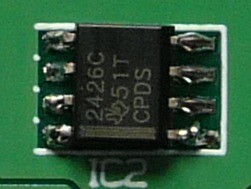 The IC 1 should have markings OP275 on it. IC1 certainly does have OP275 on it, so again no problem there. 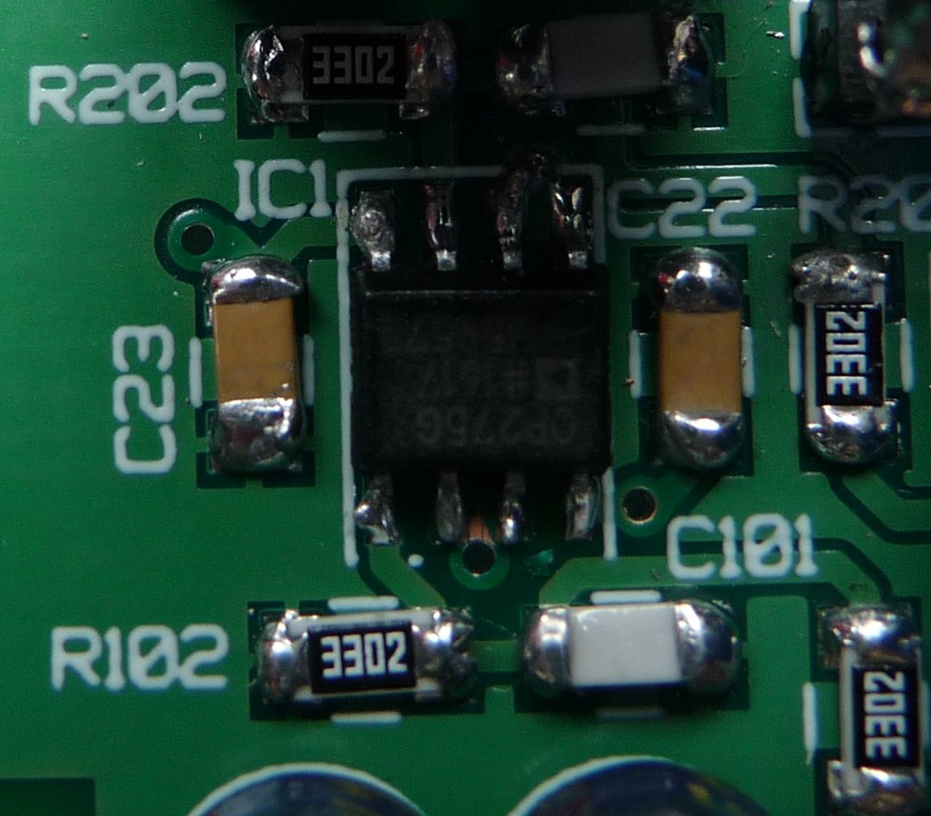 The one I sent along = IC3 (at least I thought I sent the correct opamp, 331 markings don't seem the correct part) Double checked again and it definitely has them markings? C10 - tantalum cap in place: 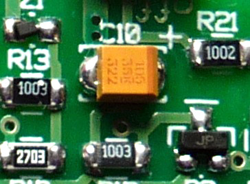 Progress with the board so far: 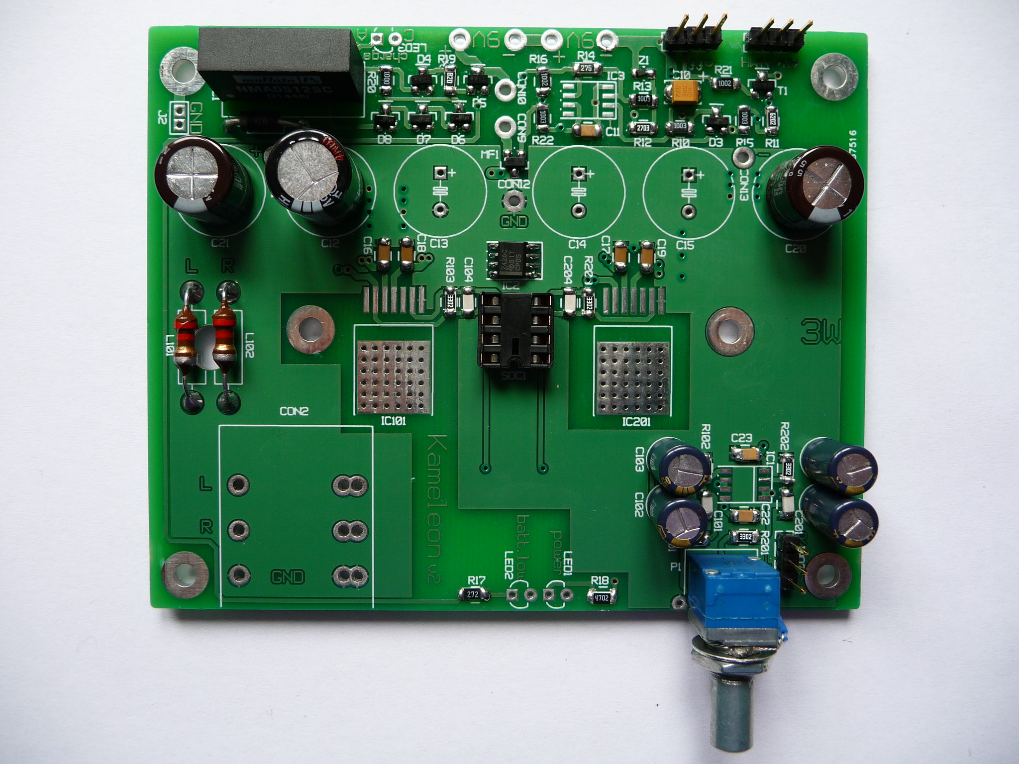 Not a great deal of soldering left to do before testing can start - just need to order a few more components first; as I go on holiday this Saturday the project will be on hold for at least 1 week  I have purposely left out C13, 14 & 15 to give me some room to solder in 1C3 when I am sure I have the correct part. |
|
Crispy
very active
Madrigal music is playing - Voices can faintly be heard, "Please leave this patient undisturbed."
Posts: 779 
|
Post by Crispy on Jun 23, 2016 14:05:52 GMT
The opamp I sent along (LT1097) for IC3 should have markings: 128 1097 It definitely does not have them markings  |
|